At Micron's memory chip fabrication facility in the Washington, DC, suburb of Manassas, Virginia, the entire manufacturing area is blanketed in electronic detectors in all their various forms. But the primary purpose isn't to keep intruders out or anything so prosaic. "A lot of them are microphones,” a spokesman for Micron said. “They listen to the robots."
It turns out that there are thousands of microphones throughout the facility, or "fab," as silicon manufacturing plants are commonly known. There are microphones inside the giant $70 million cameras that imprint the component layout on the silicon surface of a memory chip. There are microphones lining the tracks of the robot controlled railways that carry colorful plastic FOUPs (front opening universal pods) along the ceiling throughout the plant. There are microphones near essentially every moving part in the facility.
All those thousands of microphones are listening for signs of wear—for variances to develop in the noises made by the machines—so that maintenance can be scheduled before anything breaks and causes downtime. Downtime, as you might imagine, is about the worst thing that can happen to an automated chip-making facility.
Listen up
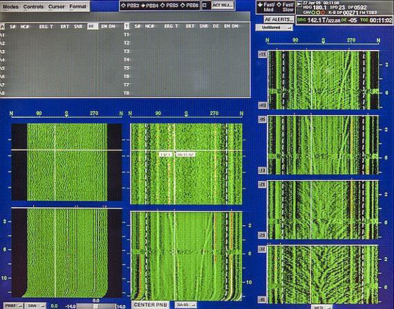
Micron engineers have created an AI system that uses deep learning to visualize the sounds produced by moving parts within the production machinery. The visualization takes place by creating a full-color time-based spectral display, which is then used by the AI software to watch for changes over time. The images resemble the sonar displays used by Navy ships and submarines to detect underwater noises.
Because each moving part has a unique sound signature, the AI software is necessary to first learn what sounds a part makes in normal operation and then to detect problems. With some time and guidance, the deep learning software can detect how badly the part is degraded—and in some cases, even diagnose what’s wrong with it.
The ability to determine the potential failure and to classify the sound signatures comes from convolutional neural networks (CNNs), which are used to extract detailed information from audio spectrographic images. The images are stored and used later as acoustic fingerprints for classification of potential problems.
Acoustics are used for more than just listening for worn bearings. Micron has also used its fab microphones to find water and air leaks and failed components by mapping the minute sounds of those leaks, along with the location from which they are emanating.
Of course, that’s not all AI does in the fab—nor are all the sensors simply arrays of microphones. A process called "real-time defect analysis" uses deep learning to perform image analysis of silicon wafers on the way to becoming memory chips. The image analysis looks for defects in the surface of the wafer, from tiny scratches to errors in the photographic process and everything else in between.
Those silicon wafers, which are actually very thin slices of a single 300 millimeter-wide silicon crystal, are the base of what will eventually be a whole batch of memory chips with electronic elements imprinted on their surfaces. Eventually the wafers are divided into an array of chips that are cut apart for individual use in products.
-
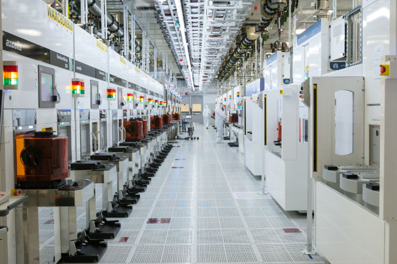
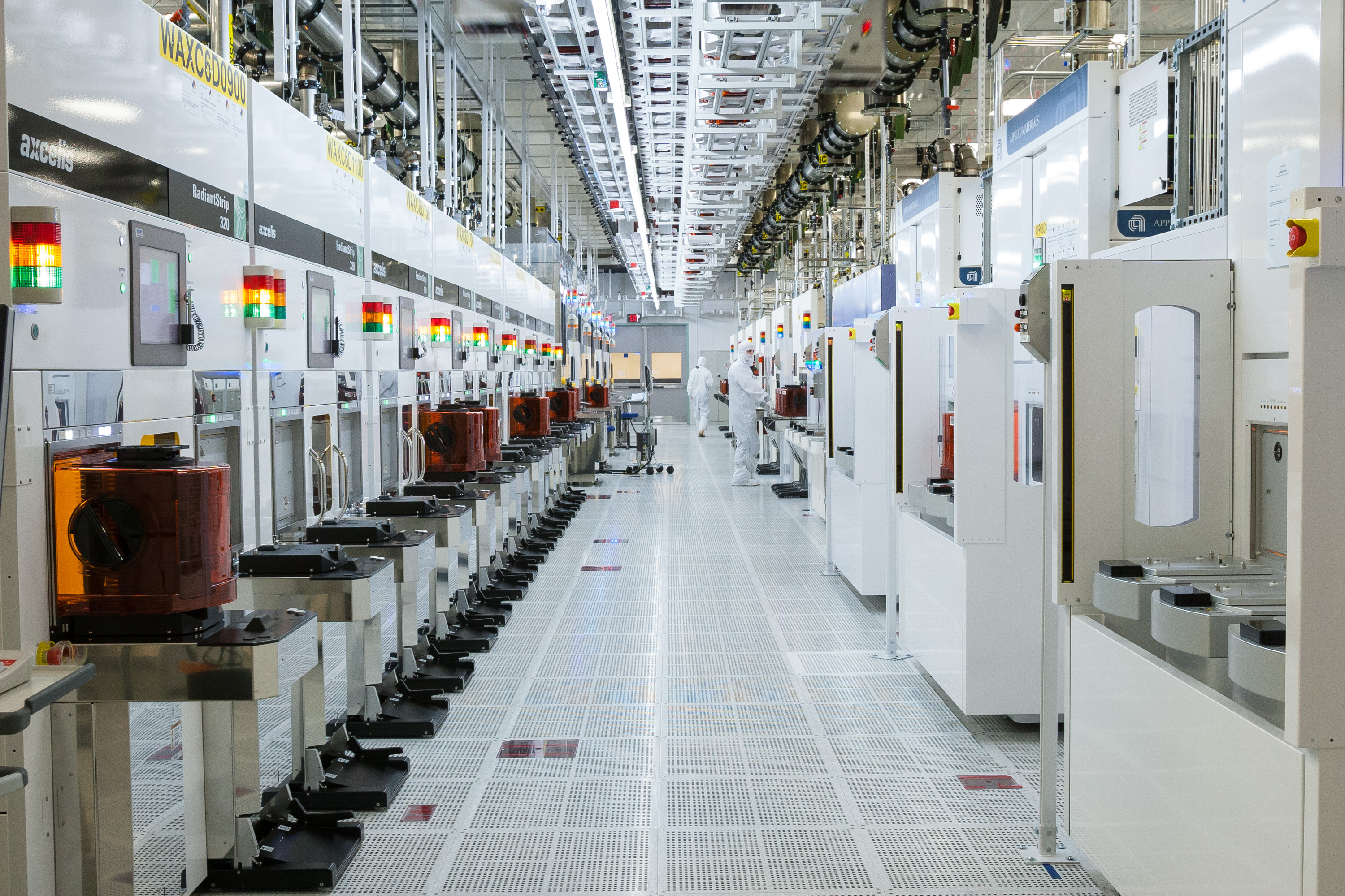
A significant portion of the Micron fab is bathed in yellow light to protect the light-sensitive coating on the wafers. Chips on the wafers are created using a photographic process. Each of the cameras, which are the machines on each side of the aisle, costs about $70 million.Micron
-
This is a Front Opening Universal Pod or FOUP. It can be either orange or green, depending on where in the manufacturing process it is, and it carries the wafers that eventually become memory chips in an automated process during manufacture.Micron
-
The FOUP rides on a carrier that travels on tracks near the ceiling, with its route being controlled by the manufacturing software. When it reaches the spot for the next manufacturing step, it drops down.Micron
-
A FOUP and the machine. The colored lights show the operational status of each machine in the manufacturing process.Micron
Augmenting people, not replacing them
Before Micron started using AI-based image analysis to find defective wafers, the job depended on people looking at the surface. As you might imagine, the visual fatigue created by this sort of a job was significant and, because of human error, was a significant problem.
By using deep learning, the image classification system can perform consistent classifications without any loss of productivity because employees start making mistakes after looking at the tiny circuits on silicon wafers for too long. Instead, the AI system learns over time, is able to accept human feedback, and can be updated with new information or classification parameters while in production.
As important as the image processing for inspecting wafers is—along with acoustic monitoring for production—the use of sensors in the fab goes far beyond those two cases. According to Micron data scientist Ted Doros, there are sensors for nearly any environmental factor you can imagine. Doros said that the company’s machine learning depends on pattern matching coupled with deep neural nets to classify wafer defects, which in turn allows the company to intelligently grade its production output. Silicon that might not meet requirements to be turned into first line "mission critical" consumer products might instead be used for less demanding things—such as electronics used in toys.
The company has also developed a series of what it calls "super sensors" that combine twelve to fourteen functions in a single package. Doros said that those functions can include vibration, temperature, humidity, or partial coronal discharge. Some sensors can detect radio frequency interference and power quality. In one case, the AI-based pattern matching was able to spot the turbulence caused by a leak in the levitation system that floats wafers on a layer of air and flag the spot for maintenance.

One unexpected set of sensors at the Manassas factory is there to monitor seismic activity. Normally, you wouldn’t think of Northern Virginia as being prone to earthquakes, but a 5.8 earthquake on August 23, 2011 knocked the fab offline for its first time ever. It turns out that quakes are more of a problem than previously expected.
“Micro quakes can ripple through the fab,” Doros explained, but with the seismic sensors in place, the AI can account for them and make adjustments in the production line.
The advanced manufacturing processes built into the Manassas fabrication plant are reflected in the plant's output. Doros said that so far, the company has seen 25% fewer quality events, along with an improvement in time to a yield of 25% and an increase in manufacturing output of 10%.
The improvement is so marked, in fact, that Micron announced in 2018 that it’s doubling the size of its Manassas fab and adding a global research center that will be used to develop even more smart manufacturing capabilities. That new facility will start coming online in stages, with the first wafers starting to appear in late 2020, Doros said.

reader comments
78